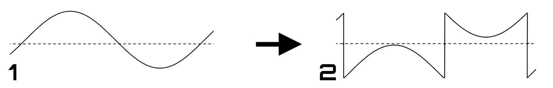
The design goal for Meg is to implement a waveshaping circuit that will shift parts of the wave up and down in this way:
It should have a low part count, need only little rack space and on top of all should be easy to build with little room for errors.
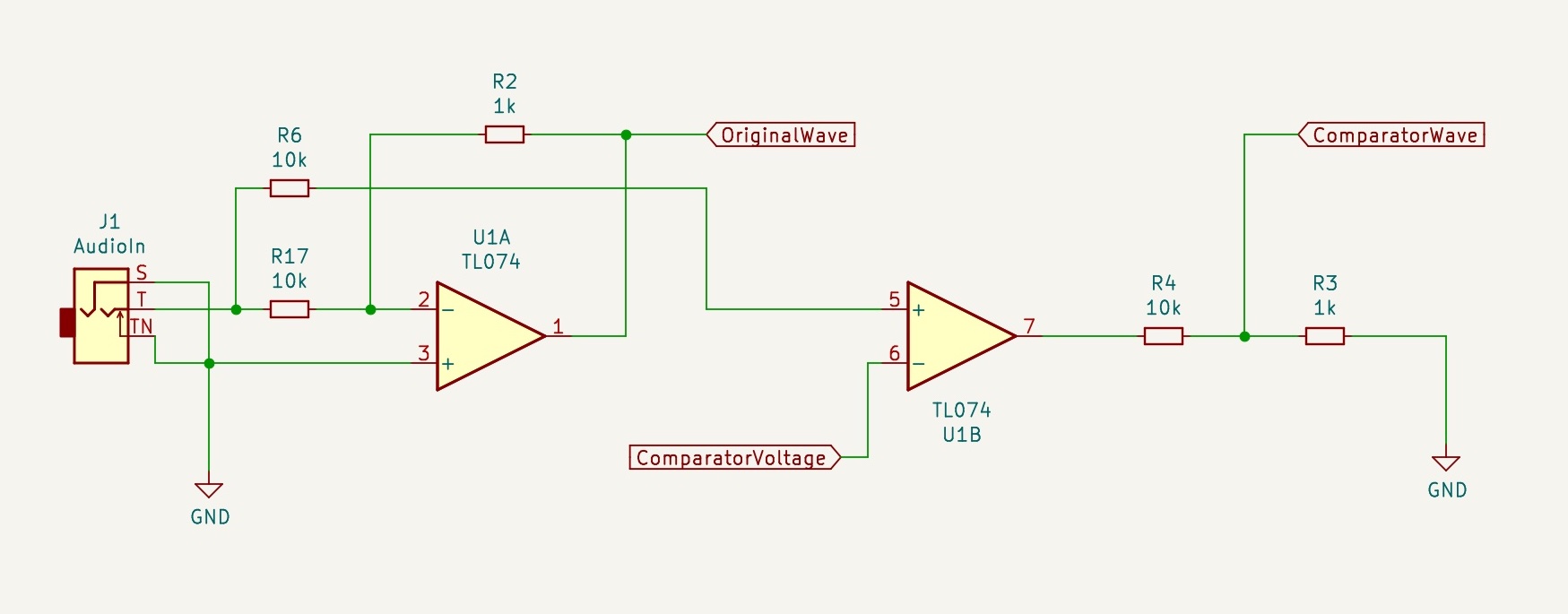
The first thing that needs to be done to the incoming audio is to buffer it, meaning we want a very high input impedance: It's possible (though unlikely) that the module that sends the incoming audio has high output impedance. Now if that was the case, and our input impedance was low, this would result in a large drop in voltage, thus not preserving the original signal. A buffer counteracts that, converting low input impedance to high input impedance. This is most commonly done using an integrated circuit called an op-amp. There are many choices for op-amps, all with different characteristics. The TL07x family is a classic in the Eurorack world (and elsewhere), and it is affordable, reliable and widely available. (This design ends up using 4 op-amps, so a single TL074 is a reasonable choice. They are represented as 4 separate units – plus the IC's power supply pins – in the schematic.)
Shifting parts of the wave can be achieved by using an op-amp in a comparator configuration. Such a comparator will compare the input voltage to a given threshold, and output either the negative supply voltage or the positive one, depending on whether the input voltage is lower or higher than the threshold. This results in a pulse wave at the output which will then be inverted and added to the original wave, giving the desired result.
A simple non-inverting buffer would not need any resistors, however, our buffer in this case shall work in a different way: For reasons that will be explained later, the signal must be attenuated. This cannot be achieved with a non-inverting op-amp configuration, as its minimum gain is 1. Hence we need an inverting op-amp circuit around U1A and will invert the signal back to the original polarity in the final op-amp stage. The ratio between the values of R2 and R17 set the gain to 0.1 (or better -0.1 since it's inverting). So an inverted signal attenuated to 10% of its original amplitude will be present at the label named OriginalWave.
The incoming signal also goes to U1B via R6. This op-amp is used in a comparator configuration, which means it compares the voltages of both its inputs and will output either the positive or negative supply voltage depending on which input is higher. (Actually, it will output a voltage slightly higher than the negative supply voltage or one that is slightly lower than the positive supply voltage, since it is not a rail-to-rail op-amp. But it's not by much and the small difference doesn't matter for our purposes.) So this op-amp compares the input signal, but to what? See this part of the circuit:
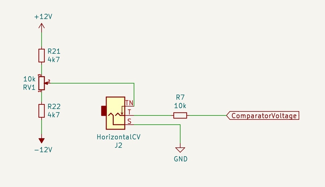
The voltage provided for comparison either comes from a CV input jack or from a potentiometer (RV1) that acts as a voltage divider between the two supply voltages. R21 and R22 set the maximum and minimum voltage that can be dialled in with RV1. If they were to be omitted, everything would still work, but since the input audio will have an amplitude smaller than 24 V (from -12 V to +12 V), there would be rather large "dead zones" at both ends of the potentiometer range, where turning it would have no effect.
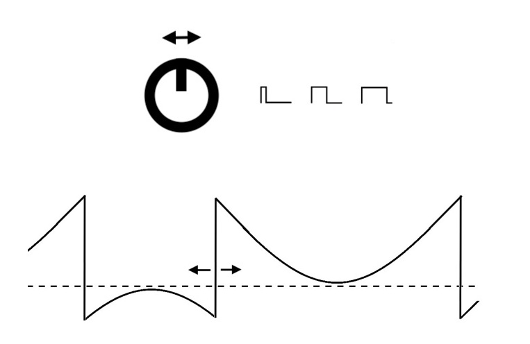
So U1B constantly compares the input signal voltage to this reference (from the pot or CV input) and outputs a very high or very low voltage, depending on whether the input signal is higher or lower than the reference. With the reference voltage at 0 V and, say, a sine signal as input, we would get a square wave, or more generally, a pulse wave. By changing this reference voltage, the user can set the point at which the wave gets shifted. For a triangle or sine wave input (as shown above), the result is basically like PWM (pulse-width modulation). For more complex waveforms, the results is equally complex in nature, and will often be sonically interesting.
Now the comparator works on the original input signal, not the inverted one. This means the pulse wave will be flipped in comparison to the inverted original. If we add the flipped pulse wave to this inverted original wave, we will get the desired waveshaping effect. We will only have to invert the resulting signal back at the module's output.
What about R3 and R4 at the comparator output? Remember that the input signal is attenuated by the input op-amp (U1A). If we're going to add the pulse wave to the attenuated signal, the pulse wave better be attenuated too, so we're not adding signals of vastly different amplitude. So R3 and R4 act as a voltage divider that attenuate the pulse signal at the label ComparatorWave to (roughly) the same amplitude as the input signal present at OriginalWave.
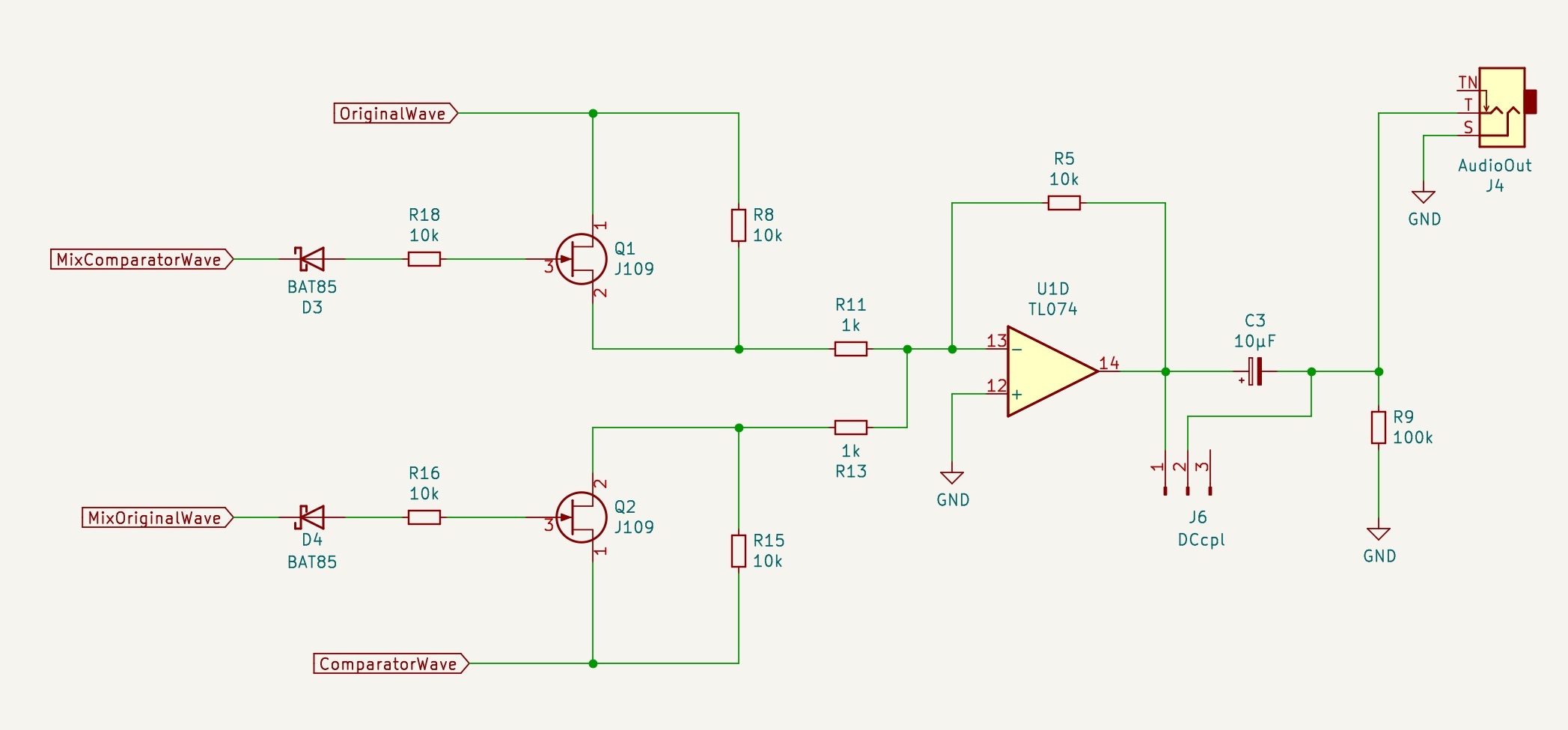
Now both of those signals need to be mixed, which is done by U1D in an inverting summing amplifier configuration. The signals are connected to its input via resistors (R11 and R13) and some more circuitry, which we will get into soon. R5 vs. the input resistance around R11 and R13 set the gain, which is now around 10 (rather -10 of course, since it's an inverting amplifier), boosting the mixed output signal back to the original level and at the same time flipping the polarity (that had previously been flipped by the input op-amp U1A).
C3 can be bypassed using the jumper on J6, making the output either AC or DC coupled. The latter means it will preserve the signal with all its low-frequency content, also DC, so this will make it feasible for CV. However, if the module is used to treat audio signals, it can be desirable – though it's not strictly necessary – to remove any DC offset or slow oscillations (below audio range). C3 and R9 form a passive high-pass filter that will do just that. In case C3 is bypassed (J6 set to DC), R9 by itself will have no perceivable effect on the output signal.
Now let's say we want some control over how OriginalWave and ComparatorWave are being mixed. We might want to be able to crossfade between both of them, meaning we would need to increase the resistance for one of the signals in the mixing circuit while simultaneously decreasing it for the other, and vice versa. This could be done with a stereo potentiometer, which would enable manual crossfading. However, this is Eurorack after all and we will of course want to have CV control. So we need a VCA (voltage controlled amplifier), or rather two of them in this case, meaning a voltage should be used to set the amplitude of the signals.
There are a couple of ways this can be done, the most popular of which is probably an operational transconductance amplifier (OTA). Using them would mean at least one more IC and space is tight. It would also be overkill for this kind of project. Some specific types of optocouplers can be used as well, such as the H11F1, which has a bilateral FET output, essentially making it a voltage controlled resistor. They are indeed underrated and are used in another Neutral Labs project (Nermal) but would again use too much space on the PCB. They can also be costly. Instead, Q1 and Q2 are JFETs (junction-gate field effect transistors) that can also act – sort of – like a voltage controlled resistor. They have a very small footprint, are affordable and do the job just fine. There is one caveat though: They only have a relatively small linear region, meaning they will not accurately map a change in voltage to a similar change in resistance if they're outside this (voltage) region. Feeding audio signals at typical Eurorack levels of +/- 5 V or even +/- 10 V would not work too well, as the output signals would be extremely distorted. This – as you may have guessed – is the reason the OriginalWave and ComparatorWave signals needed to be attenuated before going to the mixer. Now their amplitudes are small enough to be within the linear region of those JFETs.
D3 and D4 connect the JFETs to the control voltages that set the resistances. R8 and R15 are used in parallel to the JFETs Q1 and Q2 in order to make their response more predictable and linear, and set the maximum overall resistance at the same time.
But wait: In order to crossfade, we need to decrease the resistance for one signal while increasing it for the other, so how is that achieved? Have a look at this part of the circuit:
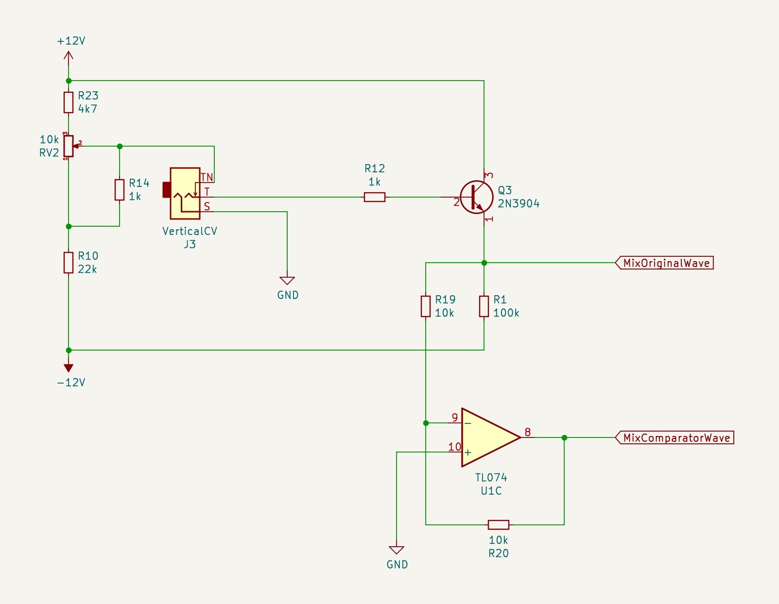
RV2 can be used to set a voltage similar to the voltage divider RV1, only the resistors around it (R10, R23) are not of the same value. This means the voltage will always be higher than the midpoint between the positive and negative supply voltage. R14 is used to change the characteristic of RV2's response curve, making it similar to the response of a logarithmic pot. When a cable is connected to J3, it will provide the control voltage instead.
R1, R12 and Q3 form a simple transistor buffer (emitter follower). This could of course easily be done by an op-amp, but since we will need U1C for another purpose and thus are out of op-amp units on the TL074, it would mean one more IC (like a TL071) plus 2 decoupling capacitors added to the project. So the general-purpose 2N3904 will do just fine. The buffered voltage is present at the label MixOriginalWave and controls the amplitude of the OriginalWave signal via Q2.
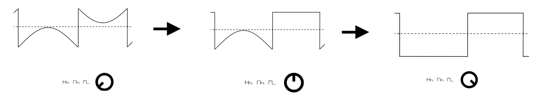
U1C is used in an inverting buffer configuration in order to invert the MixOriginalWave voltage and control MixComparatorWave via Q1. The relation between the voltage levels of these two have been chosen in such a way that the mixing circuit has a peculiar effect: While increasing the voltage, one half of the wave will be flattened first (meaning the mixing circuit will mix in more of the pulse wave signal for this half part of the wave, but not the other). Only when increasing the voltage further will the second half be gradually flattened.
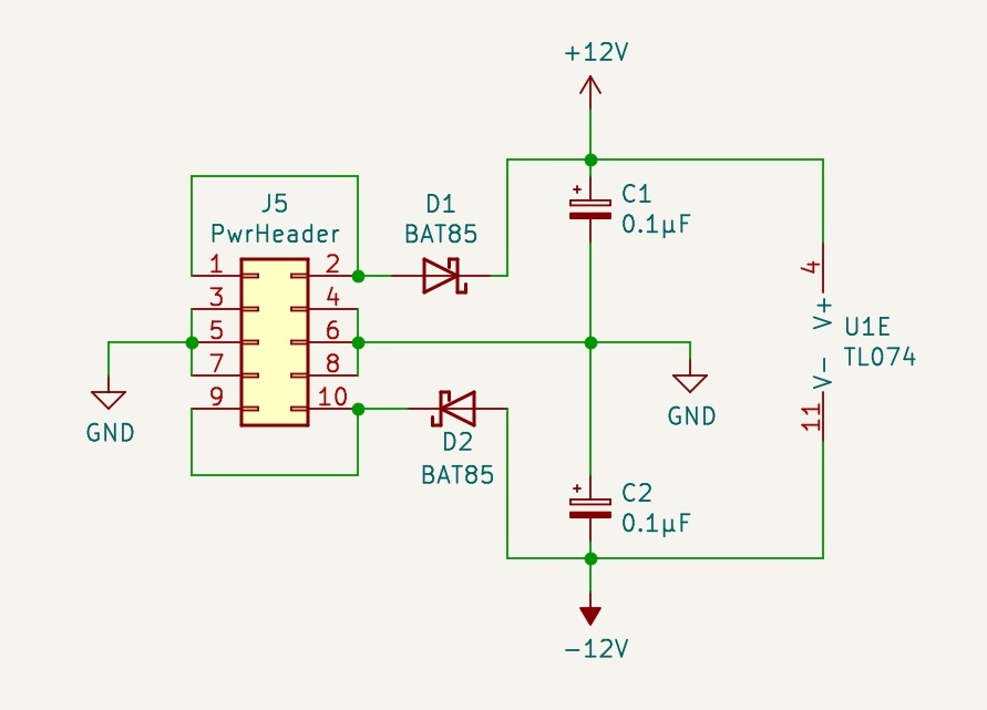
Lastly, we will of course need power to the op-amp and transistors. The power circuit in this case is very simple: We only need +12 V and -12 V as supply voltages, which we can get directly from the Eurorack power header. There are protection diodes (D1, D2) that will prevent any current from flowing in case the power cable is inserted the wrong way around. The bypass capacitors (C1, C2) will reduce any AC noise that may be present on the supply rails, which may not strictly be needed in many cases, but it is good practice, since we cannot assume the power supply will be very stable. Also, some of the op-amp units of the TL074 (U1) are driving loads to ground, which makes decoupling necessary, or at least recommended. Note the polarity: C1 has its negative leg to ground, but C2 has the positive leg to ground, since the other one is connected to -12 V. These capacitors are placed close to the power input in the schematic, but on the physical PCB they should be as close to the op-amp as possible.
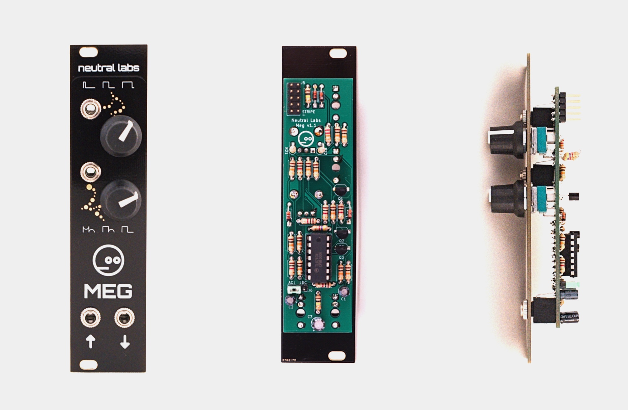
This concludes the schematic design of Meg, the unique waveshaper. See the completed module below: